 |
menu▼ |
 |
MICRO PROBER |
|
This equipment is to measure electrical characteristic for semiconductor
wafer, PCB, materials.
We provide accessories for manipulator, probe, microscopes, shield cases,
etc.
|
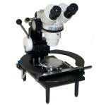 |
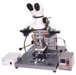
<K-157MP Simple type>
Sample size〜4 inchφ
details |
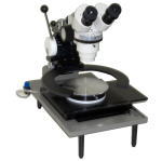 |
<K-157MP150 Simple type>
Sample size〜6 inchφ
details |
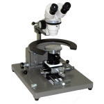 |
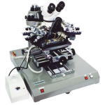
<K-160MP>
Sample size〜4 inchφ
details |
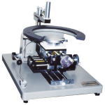 |
<K-160MW>
Sample size〜4 inchφ
details |
 |
<K-160MPH/MWH>
Sample size〜4 inchφ
with Heater stage
details |
 |
<K-163MW1>
Sample size〜6 inchφ
Both for electric driven and manual
details |
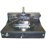 |
<K-560RM400>
Sample size〜12 inchφ/400□
details |
|
|
|
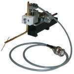
| Manipulator |
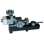
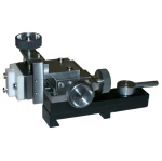
| <K-15MT> |
|
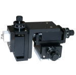
<K-15MTS> |
|
<K-15MX> |
 |
|
 |
|
 |
| X,Y,Z axes fine adjustment |
5mm 250μm/turn |
| Y axis rough adjustment |
16mm |
| θaxis rough adjustment |
90° |
| X,Y,Z axes fine adjustment mechanics |
Devetail groove mechnics
|
| Dimension |
W 38×D 120×H 65mm |
| Weight |
Approx.260g |
|
|
| X,Y,Z axes fine adjustment |
6mm 250μm/turn |
| Y axis rough adjustment |
16mm |
| θaxis rough adjustment |
90° |
| X,Y,Z axes fine adjustment mechanics |
Slide bearing mechnics |
| Dimension |
W 55×D 130×H 73mm |
| Weight |
Approx. 400g |
|
|
| X,Y,Z axes fine adjustment |
10mm 500μm/turn |
| X,Y,Z axes fine adjustment |
1mm 20μm/turn |
| X,Y,Z axes fine adjustment mechanics |
Slide bearing mechanics |
| Dimension |
W 90×D 130×H 86mm |
| Weight |
Approx. 700g |
|
|
|
| Holder & Cable |
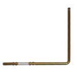
| <L type> |
|
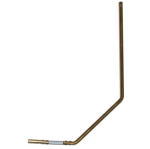
<LL type> |
|
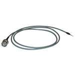
<BNC Cable> |
 |
|
 |
|
 |
|
|
| Probe |
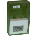 |
| Material |
Model |
size |
NeedlepointR |
| Tungsten carbide |
KM2 |
30mmL×0.7φ×10° |
2μ |
| Tungsten carbide |
KM5 |
30mmL×0.7φ×10° |
5μ |
| Tungsten carbide |
KM10 |
30mmL×0.7φ×10° |
10μ |
| Tungsten carbide |
KM30 |
30mmL×0.7φ×10° |
30μ |
| Tungsten carbideト |
KM50 |
30mmL×0.7φ×10° |
50μ |
| Silver |
KM30Ag |
30mmL×0.7φ×10° |
30μ |
| Platinum |
KM30Pt |
30mmL×0.7φ×10° |
30μ |
|
|
|
| <Example of use> |
Enlargement |
|
| UP |
|
 |
Kyowa Riken Co., Ltd. |
3-37-3 Izumi, Suginami-Ku, Tokyo 168-0063, Japan
TEL 03(3321)9911 FAX 03(3321)9917
E-MAIL:sales@kyowariken.co.jp |
|
|